![[등록] 2026-09-01 15:48:31](/support/_updata/banner2/tl181982910_6749.png)


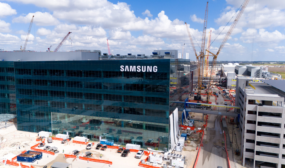
Samsung Electronics has formally announced plans to commence construction on its second semiconductor manufacturing facility in Taylor, Texas, by the end of this year. Targeting commercial mass production by 2030, the South Korean technology conglomerate is aggressively scaling up its advanced node foundry capacity to address a widening global supply shortage driven by the artificial intelligence boom.
Speaking during the company’s second-quarter earnings conference call on July 30, Samsung executive leadership revealed that current leading-edge capacity expansion is struggling to keep pace with hyper-scaling market demand. "Our current expansion rate for advanced process capacity is falling short of market demand," a Samsung spokesperson stated during the call. "To bridge this gap, we are preparing to break ground on Taylor Fab 2 by the end of this year, with an eye toward achieving mass production by 2030."
Taylor Fab 1 Progress and 2-Nanometer Roadmap
While Fab 2 enters its initial construction phase, work on Samsung's flagship Taylor Fab 1 remains fully on schedule to begin operations in 2026. Designed as the anchor facility for Samsung's $44 billion-plus mega-cluster in Williamson County, Texas, Fab 1 will serve as the premier Western manufacturing hub for the company’s 2-nanometer (SF2) process technology.
Following its initial operational debut, Samsung plans a phased, multi-stage capacity expansion for 2nm production at Fab 1. Utilizing its proprietary Gate-All-Around (GAA) Multi-Bridge-Channel FET (MBCFET) architecture—which Samsung pioneered commercially at the 3nm node—the Taylor facility aims to offer global fabless customers high-yield, power-efficient chips tailored for high-performance computing (HPC), mobile processors, and specialized AI hardware acceleration.
Inquiries Surge for 1.4nm (SF1.4) Next-Generation Nodes
In addition to committing to Fab 2, Samsung confirmed for the first time that it is actively evaluating the construction of supplementary manufacturing facilities specifically dedicated to its upcoming 1.4-nanometer process node (SF1.4). The move comes in response to an unprecedented influx of client requests from major global tech firms seeking guaranteed capacity for sub-2nm fabrication toward the end of the decade.
"Customer inquiries regarding the 1.4nm node have increased substantially," Samsung stated during the earnings briefing. "Consequently, we are evaluating options for additional fab capacity. Concrete investment plans will be finalized sequentially based on ongoing customer contract negotiations and order commitments."
Strategic Restructuring: Pivot to Specialty & High-Margin 3-Tier Nodes
Alongside its aggressive capital expenditure on leading-edge sub-2nm nodes, Samsung is executing a sweeping operational shift across its legacy and mature node foundries. Rather than engaging in low-margin price wars for commoditized legacy logic, Samsung is pivoting its mature node strategy strictly toward high-profitability, specialized applications.
Under this revised operational model, Samsung will systematically reduce the proportion of standard, general-purpose commoditized logic chips. Instead, the company is reallocating mature capacity toward high-value 3-tier processes and specialized specialty technology platforms. These include embedded magnetoresistive RAM (eMRAM), high-frequency radio frequency (RF) ICs, advanced power management integrated circuits (PMICs), and high-resolution image sensors—sectors with high technological entry barriers and resilient pricing power.
Global Foundry & CHIPS Act Strategic Context
US CHIPS Act Support: Samsung's Taylor expansion is anchored by up to $6.4 billion in direct federal subsidies from the U.S. Department of Commerce under the CHIPS and Science Act.
Tri-Polar Foundry Competition: Samsung continues its fierce rivalry with TSMC (which is building three fabs in Phoenix, Arizona) and Intel Foundry Services (IFS) for dominance in North American leading-edge manufacturing.
AI Infrastructure Crunch: Hyper-scalers (including Google, Microsoft, Meta, and Amazon) and chip designers (such as NVIDIA and AMD) are locking in advanced node capacity years in advance to secure AI accelerator supply.
Advanced Packaging Integration: Samsung is pairing its Taylor leading-edge foundry nodes with turnkey advanced 2.5D/3D packaging solutions (I-Cube/SAINT) to offer unified front-end and back-end services.
Industry Impact and Competitive Dynamics
Samsung’s double-down on Taylor comes at a pivotal juncture for the semiconductor industry. As tech giants race to deploy increasingly sophisticated generative AI models, the demand for wafer fabrication at 3nm, 2nm, and eventually 1.4nm has created severe bottlenecks across global supply chains. TSMC's advanced capacity remains heavily booked, prompting fabless customers to diversify their supply sources and seek secondary manufacturing partners in North America.
By establishing a robust, multi-fab footprint in Texas—backed by $6.4 billion in U.S. CHIPS Act incentives—Samsung is positioning itself as an indispensable alternative for U.S.-based chip designers seeking geographic supply chain resilience without compromising on process performance.
Industry analysts note that while the 2030 target for Fab 2 represents a long-term horizon, the early groundbreaking demonstrates Samsung's commitment to securing civil engineering, cleanroom infrastructure, and long-lead extreme ultraviolet (EUV) lithography tools well ahead of full-scale equipment installation. As negotiations for 1.4nm orders intensity throughout 2026 and 2027, Samsung's expanded Taylor cluster could prove instrumental in reshaping the global foundry balance of power.
[Copyright (c) Global Economic Times. All Rights Reserved.]